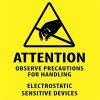
 In my research of the technical forums, I have not found this subject addressed, so I thought I would offer a few words in order to provide a little information that may improve the life of your electronic components (EHC, Control Boards, etc.) found in your Big Dog Motorcycle, or any other electronic device you work on for that matter.
In this age of printed circuit boards, special handling procedures will greatly reduce component failures due to the damage caused by the inadvertent exposure of the extremely thin circuit paths between components on the board to electrostatic discharge (ESD) with a few simple precautions.
These paths are very thin and inherently susceptible to the effects of as low as 50 volts of static electricity.
To put this into perspective, when a person walks across a carpet and then touches a grounded object, the resulting discharge is at least 2,000 volts @ microamperage, in order to be perceptible, or felt.
Touching the connectors or contact portion of any circuit board, when a difference in potential is present, will introduce this voltage through the thin ribbons of conductive matetial used as circuit paths. The resulting damage may immediately destroy the path, or may simply weaken it, leading to componet failure at a later date (latent ESD damage) under normal operating conditions, and the user will not even be aware the discharge has taken place.
There are two simple precautions you can take to reduce or eliminate the chances of this occuring.
1. Ground yourself using properly grounded and applied ESD wrist strap. This will discharge any potential.
2. Avoid touching the contact paddles or connector surfaces of your components.
The electrical theory and applied science involved are quite extensive, and too deep to delve into here, but available for review with a search of the subject on Google.
Hope some of you will find this useful and informative.
Last edited:


